
AML Wafer Bonder
Description
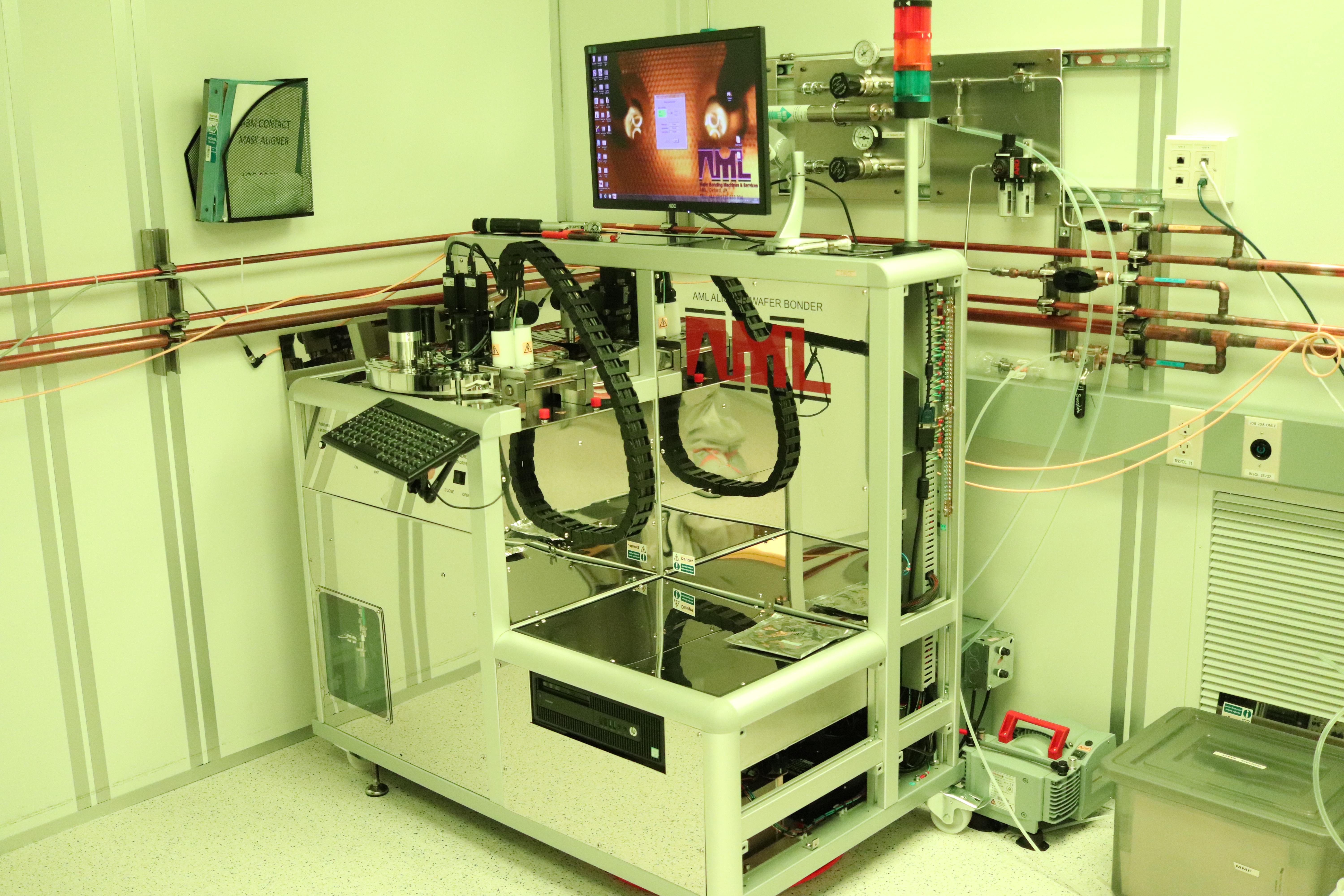
The AML Aligner Wafer Bonder (AWB) is used to bond two wafers together for micro electromechanical systems (MEMS), microfluidic systems, or various other applications. Bonding processes that are possible on the AWB include anodic, adhesive, or eutectic bonding. These processes typically use pressure, force, and heat, together with either high voltages, adhesives materials, and/or annealing to join two wafers. Specifically, anodic bonding relies on high voltage to induce ion migration between a glass and silicon wafer, forming covalent bonds at elevated temperatures. Adhesive bonding utilizes an intermediate adhesive material to form strong bonds between wafers under controlled pressure and temperature. Finally, eutectic bonding typically involves melting a thin layer of material between two wafers at high temperatures, allowing them to join upon solidification, which will form a strong metallic alloy/bond. This equipment offers several advantages over traditional bonding methods, including precise bonding parameter controls, cost-effectiveness, and precision alignment features. Given the involvement of high voltages, heat, pressure, and force, it is crucial to follow all safety protocols during operation.