KMPR 1010 Procedure
- Plasma Cleaning: Place glass wafer in PVA Tepla Ion 10 and select the “Omnicoat lift up” recipe to ash the wafer. Edit the recipe and set plasma ignite to 5 minutes. This will clean the wafer and ensure better adhesion later in the process.
- Dehydration: Dehydrate wafer on hot plate for 5 minutes at 150° C. After dehydration bake allow wafer to cool to room temperature.
- HMDS Coating: Use the Brewer Spin Coater with the following profile:
- Speed: 250 RPM, Ramp: 250 RPM/s, Time: 5 seconds
- Speed: 2000 RPM, Ramp: 700 RPM/s, Time: 35 seconds
- Speed: 0 RPM, Ramp: 1000 RPM/s, Time: 7 seconds
- After HMDS spin, the wafer should look dry and clean. Remove the wafer from the chuck and rinse the bowl with acetone to remove the HMDS spill.
- Cover the bowl of the Brewer Spin coater with Aluminum foil to avoid photoresist contact spill.
- Place the wafer back on chuck and pour 15 to 20 mL of KMPR 1010 into center of wafer (this should cover more than 2/3 of the wafers surface).
- KMPR Coating: Use the following recipe on the spin coater:
- Speed: 500 RPM, Ramp: 100 RPM/s, Time: 12 seconds
- Speed: 2000 RPM, Ramp: 700 RPM/s, Time: 35 seconds
- Speed: 3500 RPM, Ramp: 1000 RPM/s, Time: 7 seconds
- Speed: 0 RPM, Ramp: 500 RPM/s, Time: 5 seconds
- Soft Bake: Being careful not to tilt the photoresist coated wafer, remove the wafer from the spinner and soft bake wafer on hot plate for 7 minutes at 100° C. After soft bake allow wafer to cool to room temperature before continuing process.
- Insert i-line (365nm) filter into contact aligner. Open the nitrogen and vacuum valves to the right of the contact aligner.
- Measure the intensity of contact aligner at each of the four corners of the stage as well as the center and take the average intensity.
- Contact Alignment: Place wafer on the contact aligner substrate stage. Be sure to confirm that the substrate stage is below the mask stage. Place the lithography mask onto the mask stage and turn the mask vacuum and nitrogen flow on. While depressing the leveling chuck, raise the stage until relatively hard contact is made between the mask and wafer and turn the contact vacuum on.
- Exposure: Expose wafer so that the total intensity seen by the wafer is 410 mJ. To calculate exposure time, take 410 mJ and divide it by number of exposures and measured intensity. Exposures should be less than 15 seconds due to the fragile nature of the photoresist and should allow 30 seconds in between exposures to allow photoresist to cool.
- Turn contact vacuum and nitrogen flow off. Lower the substrate stage, turn off the mask vacuum and remove the lithography mask. Now turn off the substrate vacuum.
- Hard Bake: Remove the wafer and place on a hot plate to hard bake the wafer for 2 minutes at 100° C. After hard bake allow wafer to cool to room temperature.
- Development: Develop wafer pattern face up for 45 seconds in AZ300 MIF developer, transfer wafer to a water bath for 30 seconds, and then finally a second water bath for 15 seconds.
- Dry with nitrogen gun.
- Develop further as desired.
Result Expectation:
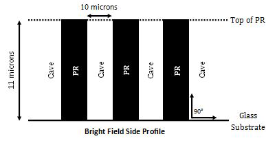
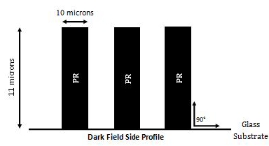
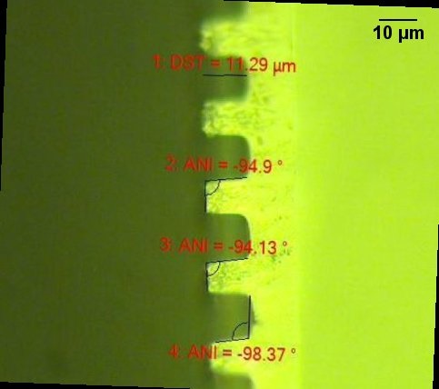
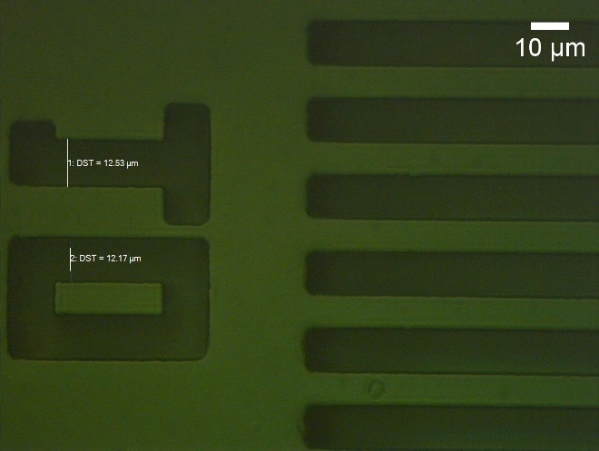
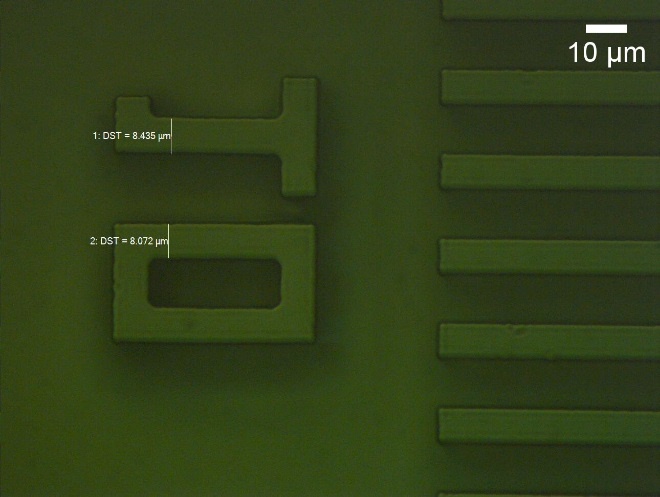
For pattern dimensions larger than or equal to 10 micrometers in width and 11 microns in height, angles of approximately 95 degrees between photoresist and substrate can be achieved.
Bright Field 100x
Dark Field 100x