AZ 1512 Procedure
- Start from a clean wafer.
- Dehydration: 120°C baking for 10 mins.
- Adhesive promotor coating: Programmed HMDS coating (Program 1).
- Spin Coating: Note. To ensure adhesive promotor active, start PR spin coating right after HMDS coating.
- Dispense sufficient amount of AZ 1512 from the center of the wafer covering 60% -
70%
of the wafer surface. - Spin at 500 rpm for 20 seconds to spread out the photoresist.
- Spin at 4000 rpm for 35 seconds to reach 1.3 micrometer in thickness. (+ or – 476 nm).
- Dispense sufficient amount of AZ 1512 from the center of the wafer covering 60% -
70%
- Soft Bake: 110°C (1 min).
- Exposure: 2.4 seconds with expose dose 40 mJ.
- Develop:
- 50 seconds gentle agitation in AZ 300MIF solution.
- (Optional) Stir the wafer slightly to remove red PR residue floating on top of wafer.
- Rinsing: Dip into water to remove developer.
- Dry: Blow dry the wafer with compressed Nitrogen gun.
Result Expectation:
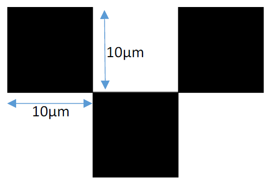
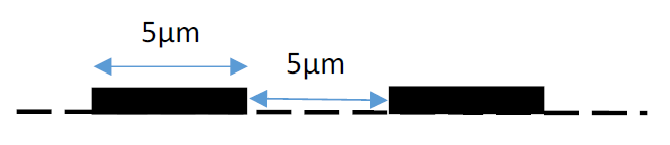
For pattern dimension larger or equal to 2 micrometers, single layer pattern has 75°
or higher cross-sectional
angle at the silicon substrate.